XiaoMi-AI文件搜索系统
World File Search SystemCHAdeMO
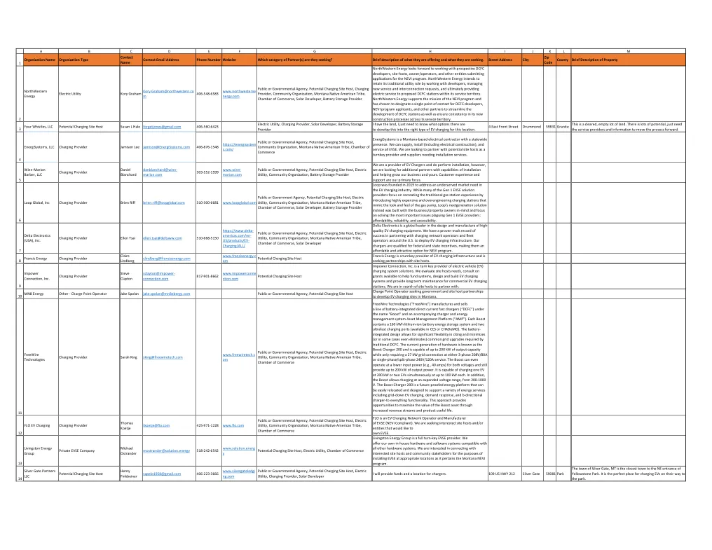
蒙大拿州国家电动汽车基础设施合作伙伴清单
FreeWire Technologies(“ FreeWire”)以“ Boost”的名称以及随附的充电器和能源管理系统资产管理平台(“ AMP”)制造并出售一系列电池集成的直流快速充电器(“ DCFC”)。每个提升都包含一个160 kWh锂离子电池储能系统和两个超快充电端口(可在CCS或Chademo中使用)。电池集成的设计允许引用和最小化(或在某些情况下消除)传统DCFC所需的常见网格升级。当前的硬件被称为Boost Charger 200,并且能够达到200 kW的输出能力,而仅在3相208V/80A或单相/单相/拆分相240V/120A服务下仅需要27 kW网格连接。这两种电压甚至可以以较低的输入功率(例如40安培)以较低的输入功率运行,并且仍然提供多达200 kW的输出功率。它能够同时在200 kW或两台电动汽车上以每人100 kW的速度同时收取1 ev。此外,增强功能允许在200-1000 V的扩展电压范围内充电。BoostCharger 200是一个未来的能源平台,可以轻松地搬迁并设计以支持各种能源服务,包括网格降低电动汽车充电,需求响应,需求响应以及B方向充电器到所有功能。这种方法提供了通过增加收入流和产品有用寿命来最大化增长资产价值的机会。
使用日产叶的车辆到负载系统的设计和模拟
图3-11:MATLAB SIMULINK模拟设计的电池。 .................... 40 Figure 3-12 MATLAB SIMULINK simulation of battery comparison. ................. 41 Figure 3-13: SOC results of comparison simulation................................................ 42 Figure 3-14: OCV results of first order RC batteries comparison. ...............................................................................................................................................................................................................................................................................................................................................................................................二阶RC电池比较的OCV结果。 ..................... 43 Figure 4-1 Traditional bridge-type PWM inverter. (a)拓扑。 (b)波形[30]。 .......................................................................................................................... 45 Figure 4-2 LC Filter equivalent circuit. ................................................................... 46 Figure 4-3: The V2L electrical circuit. .................................................................... 49 Figure 4-4: The equivalent circuit of the V2L system. ............................................ 49 Figure 4-5 Bode Plot of the voltage plant. ............................................................... 52 Figure 4-6: Bode Plot of the current plant. .............................................................. 53 Figure 4-7 the block diagram of the outer voltage control loop with the inner current loop. .......................................................................................................................... 54 Figure 4-8: MATLAB SIMULINK simulation of complete system. .................................................... 57 Figure 4-11 Inductor current result of the system. 。图3-11:MATLAB SIMULINK模拟设计的电池。.................... 40 Figure 3-12 MATLAB SIMULINK simulation of battery comparison.................. 41 Figure 3-13: SOC results of comparison simulation................................................ 42 Figure 3-14: OCV results of first order RC batteries comparison................................................................................................................................................................................................................................................................................................................................................................................................二阶RC电池比较的OCV结果。 ..................... 43 Figure 4-1 Traditional bridge-type PWM inverter. (a)拓扑。 (b)波形[30]。 .......................................................................................................................... 45 Figure 4-2 LC Filter equivalent circuit. ................................................................... 46 Figure 4-3: The V2L electrical circuit. .................................................................... 49 Figure 4-4: The equivalent circuit of the V2L system. ............................................ 49 Figure 4-5 Bode Plot of the voltage plant. ............................................................... 52 Figure 4-6: Bode Plot of the current plant. .............................................................. 53 Figure 4-7 the block diagram of the outer voltage control loop with the inner current loop. .......................................................................................................................... 54 Figure 4-8: MATLAB SIMULINK simulation of complete system. .................................................... 57 Figure 4-11 Inductor current result of the system. 。...............................................................................................................................................................................................................................................................................................................................................................................................二阶RC电池比较的OCV结果。..................... 43 Figure 4-1 Traditional bridge-type PWM inverter.(a)拓扑。(b)波形[30]。.......................................................................................................................... 45 Figure 4-2 LC Filter equivalent circuit.................................................................... 46 Figure 4-3: The V2L electrical circuit..................................................................... 49 Figure 4-4: The equivalent circuit of the V2L system............................................. 49 Figure 4-5 Bode Plot of the voltage plant................................................................ 52 Figure 4-6: Bode Plot of the current plant............................................................... 53 Figure 4-7 the block diagram of the outer voltage control loop with the inner current loop........................................................................................................................... 54 Figure 4-8: MATLAB SIMULINK simulation of complete system..................................................... 57 Figure 4-11 Inductor current result of the system.。...................... 55 Figure 4-9: Output voltage result of the system....................................................... 56 Figure 4-10: Output current result of the system.................................................... 57 Figure 4-12: PWM Waveforms of the system.............................................................................................................................................................................................................................................................................................................................................................................................................................................................................. 58图4-14输出和参考电压....................................................................................................................................... 60 Figure 5-2: Experimental Setup............................................................................... 61 Figure 5-3: Experimental setup; (1)variac,(2)3-φ整流器,(3)控制器,(4)电阻载荷,(5)逆变器,(6)DSP板和电平换挡器电路,(7)示波器,(8)LC滤波器。..................................................................................... 61 Figure 5-4: The connection diagram of the F28335 processor and the level shifter................................................................................................................................... 63 Figure 5-5: Experimental Setup Connection of DSP board and the Level Shifter.64图5-6:无过滤器的逆变器的输出电压。...................................... 65 Figure 5-7: Load voltage and current....................................................................... 66 Figure 5-8: Load Voltage.............................................................................................................................................................................. 71........................................................................................ 66 Figure 5-9 Transient Current and Voltage of Kettle ................................................ 67 Figure 5-10 Transient Current and Voltage of Microwave ..................................... 67 Figure 5-11 Steady-State Current and Voltage of Kettle ......................................... 68 Figure 5-12 Steady-State Current and Voltage of Microwave ................................ 68 Figure 6-1 CHAdeMO Connector and Pin Layout [45].