XiaoMi-AI文件搜索系统
World File Search SystemDRV
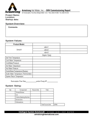
Armstrong Hot Water,Inc。 - DRV调试报告
如果原发电源故障定期发生,或者将DRV安装在安全系统中,该供应系统至关重要,则必须至少每12个月更换一次电池,作为年度维护例程的一部分。在非关键系统中或电池使用率低,更长的替换周期最多可被视为最多5年。

1,以抗第五代蛋白酶抑制剂...
摘要Darunavir(DRV)在高药物浓度的有效HIV-1蛋白酶抑制剂(PI)中是在体内实现的。对DRV的从头抗性途径知之甚少。我们选择了对10个PI及其结构前体DRV的高药物浓度的抗性。突变通过两种途径积累(由蛋白酶突变I50V或I84V锚定)。抑制剂P1'-等效位置的小变化导致优先使用一种途径而不是另一种途径。抑制剂P2'-等效位置的变化确定了在抗性病毒中保留的效力的差异,并影响了所选突变。病毒变异显示了插科打裂解部位的补偿性突变的不同选择。这些结果揭示了第五代PI可以达到的高水平选择压力,以及抑制剂的特征如何影响电阻途径和面对电阻时的剩余效力。

1,以抗第五代蛋白酶抑制剂...
摘要darunavir(DRV)在高药物浓度的有效HIV-1蛋白酶抑制剂(PI)中是在体内实现的。对DRV的从头抗性途径知之甚少。我们选择了对10个PI及其结构前体DRV的高药物浓度的抗性。突变通过两种途径积累(由蛋白酶突变I50V或I84V锚定)。抑制剂P1'-等效位置的小变化导致优先使用一种途径而不是另一种途径。抑制剂P2'-等效位置的变化确定了在抗性病毒中保留的效力的差异,并影响了所选突变。病毒变异显示了插科打裂解部位的补偿性突变的不同选择。这些结果揭示了第五代PI可以达到的高水平选择压力,以及抑制剂的特征如何影响电阻途径和面对电阻时的剩余效力。
大脑网络安装和操作指南
DRV产品是一种微处理器控制的再循环阀,专门用于温水系统。冷水混合在一起,以在阀的配置软件中存储的设定点产生混合水。为了有效地执行此操作,它具有3个温度传感器,可以不断监视热入口,冷入口和出口(混合)温度。DRV产品旨在为了安全起见,旨在在所选的设定点上自动保持水温。规定如果出口温度落在某些操作参数之外,则产生各种警报和错误条件:
Brain®Modbus网络安装指南和...
DRV产品是一种微处理器控制的再循环阀,专门用于温水系统。冷水混合在一起,以在阀的配置软件中存储的设定点产生混合水。为了有效地执行此操作,它具有3个温度传感器,可以不断监视热入口,冷入口和出口(混合)温度。DRV产品旨在为了安全起见,旨在在所选的设定点上自动保持水温。规定如果出口温度落在某些操作参数之外,则产生各种警报和错误条件:

开始什么:基于蛋白酶的基于蛋白酶的方案
The U.S. Food and Drug Administration (FDA)–approved protease inhibitors (PIs) include atazanavir (ATV), atazanavir/cobicistat (ATV/c), darunavir (DRV), darunavir/cobicistat (DRV/c), fosamprenavir (FPV), indinavir (IDV), lopinavir/ritonavir (LPV/R),Nelfinavir(NFV),Ritonavir(RTV),Saquinavir(SQV)和Tipranavir(TPV)。使用Cobicistat(Cobi)或RTV(也称为PK升高)的药代动力学(PK)增强的基于PI的方案(PK)会增加浓度并延长PI的半衰期。这些方案表现出病毒学效力,艺术性人士的耐用性以及耐药性的高障碍。因为LPV/R,Fosamprenavir/Ritonavir(FPV/R),ATV(有或没有PK增强剂)和Saquinavir/Ritonavir(SQV/R)具有缺点,例如较大的药丸负担,较大的药丸负担,较低的疗效,毒性较低,毒性增加了两种毒性,或者毒性增加了两种成分的driprient,又是一定效率的drivition invirention n comprient invirention -n contriend comprient invers compriention compriention compriention compriention -n contriend comprient comprient invers-在某些临床情况下,建议(NRTIS)作为初始治疗(请参见HIV患者的初始组合抗逆转录病毒方案的表6B)。

FBS-GAM01P-R-PSE
双向电源良好 (PG) 输出和关断 (*SD) 输入引脚。要从外部禁用 FBS-GAM01P-R-PSE(将 OUT 引脚强制为低 (OFF) 状态),应将 SD/PG 引脚连接到逻辑地,例如通过开漏/集电极。该模块还包含一个电源良好 (PG) 感应电路,当 +5 V DC 栅极驱动偏置电位 (V BIAS ) 低于“PG 功能静态电气特性”表(见第 4 页)中指定的欠压阈值范围时,该电路将禁用驱动器。在 V BIAS 电位低于预设阈值期间,PG 输出(引脚 5)引脚通过开漏拉低(至 LGND)。或者,当 V BIAS 电位高于预设阈值时,PG 引脚通过外部上拉电阻拉高至 V DRV 。为了正常运行,应使用 4.7 kΩ 电阻将引脚 9 外部上拉至 V DRV (引脚 3)。
记录计划(POR)文档模板
记录POR部署就绪(PORDR)日期。这是客户实验室和/或现场测试完成的日期,并且客户认为软件被视为开始在其余目标设备中安装。这是在完成实际部署现成里程碑后,将用于确定部署现成方差(DRV)度量的日期。POR部署准备(PORDR)日期:mm/dd/yyyy