XiaoMi-AI文件搜索系统
World File Search SystemTechnology
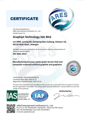
GraphJet Technology SDN BHD
每次监视审核与最后一次现场审核之间的时间间隔不得超过12个月,并且组织必须获得ARES发布的“监视审计批准通知”,以确保证书的有效性。

CBAK Energy Technology,Inc。
本演讲包含1995年《私人证券诉讼改革法案法》的含义中的前瞻性陈述,包括,包括而不用限制,暗示和明示有关Nuvalent的战略,业务计划和重点的陈述; Nuvalent估计其现金,现金同等和可销售证券的期限足以为其未来的运营支出和资本支出要求提供资金;数据公告的预期时间; NVL-520,NVL-655和NVL-330的临床前和临床开发计划; NVL-520,NVL-655和NVL-330的潜在临床和临床前效应; ARROS-1和ALKOVE-1试验的设计和注册,包括ARROS-1的预期注册指导设计; Nuvalent管道计划的潜力,包括NVL-520,NVL-655和NVL-330;数据读数和演示; Nuvent的癌症治疗的研发计划;以及与药物开发相关的风险和不确定性。The words “may,” “might,” “will,” “could,” “would,” “should,” “expect,” “plan,” “anticipate,” “aim,” “goal,” “intend,” “believe,” “expect,” “estimate,” “seek,” “predict,” “future,” “project,” “potential,” “continue,” “target” or the negative of these terms and similar words or expressions are intended to identify forward-looking语句,尽管并非所有前瞻性语句都包含这些识别单词。药物开发和商业化涉及高风险,只有少量的研发计划才会导致产品商业化。您不应过分依赖这些陈述或提出的科学数据。
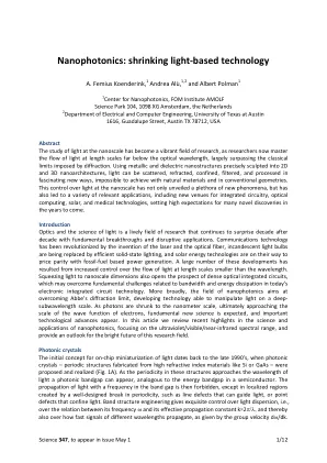
Nanophotonics: shrinking light-based technology
Abstract The study of light at the nanoscale has become a vibrant field of research, as researchers now master the flow of light at length scales far below the optical wavelength, largely surpassing the classical limits imposed by diffraction. Using metallic and dielectric nanostructures precisely sculpted into 2D and 3D nanoarchitectures, light can be scattered, refracted, confined, filtered, and processed in fascinating new ways, impossible to achieve with natural materials and in conventional geometries. This control over light at the nanoscale has not only unveiled a plethora of new phenomena, but has also led to a variety of relevant applications, including new venues for integrated circuitry, optical computing, solar, and medical technologies, setting high expectations for many novel discoveries in the years to come. Introduction Optics and the science of light is a lively field of research that continues to surprise decade after decade with fundamental breakthroughs and disruptive applications. Communications technology has been revolutionized by the invention of the laser and the optical fiber, incandescent light bulbs are being replaced by efficient solid-state lighting, and solar energy technologies are on their way to price parity with fossil-fuel based power generation. A large number of these developments has resulted from increased control over the flow of light at length scales smaller than the wavelength. Squeezing light to nanoscale dimensions also opens the prospect of dense optical integrated circuits, which may overcome fundamental challenges related to bandwidth and energy dissipation in today's electronic integrated circuit technology. More broadly, the field of nanophotonics aims at overcoming Abbe's diffraction limit, developing technology able to manipulate light on a deep- subwavelength scale. As photons are shrunk to the nanometer scale, ultimately approaching the scale of the wave function of electrons, fundamental new science is expected, and important technological advances appear. In this article we review recent highlights in the science and applications of nanophotonics, focusing on the ultraviolet/visible/near-infrared spectral range, and provide an outlook for the bright future of this research field. Photonic crystals The initial concept for on-chip miniaturization of light dates back to the late 1990's, when photonic crystals – periodic structures fabricated from high refractive index materials like Si or GaAs – were proposed and realized (Fig. 1A). As the periodicity in these structures approaches the wavelength of light a photonic bandgap can appear, analogous to the energy bandgap in a semiconductor. The propagation of light with a frequency in the band gap is then forbidden, except in localized regions created by a well-designed break in periodicity, such as line defects that can guide light, or point defects that confine light. Band structure engineering gives exquisite control over light dispersion, i.e., over the relation between its frequency ω and its effective propagation constant k=2 π/λ, and thereby also over how fast signals of different wavelengths propagate, as given by the group velocity d ω /dk.
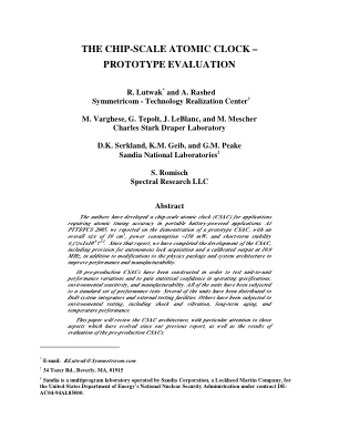
芯片级原子钟 - Microchip Technology
第三阶段物理组件(上图 1(b))保留了第二阶段设计的许多成功特性(来自 [3],如图 1(a) 所示)。加热谐振单元组件由张紧聚酰亚胺“系绳”支撑,这些系绳在机械坚固的配置中提供非凡的热隔离(7000°C/W)。使用传统的光刻技术将谐振单元组件的电气连接以及加热器本身图案化到聚酰亚胺上,以便(导热、金属)迹线的尺寸由电气要求而非机械要求决定,从而最大限度地减少通过电子连接的热损失。共振腔本身由 Pyrex ® 窗口阳极键合到穿孔硅晶片制成,除了温度补偿缓冲气体混合物外,还含有少量金属铯,从第二阶段到第三阶段的演变过程中也没有变化。
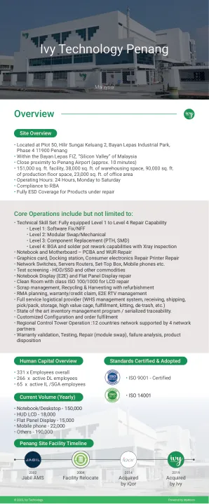
Ivy Technology槟城
• Technical Skill Set: Fully equipped Level 1 to Level 4 Repair Capability • Level 1: Software Fix/NFF • Level 2: Modular Swap/Mechanical • Level 3: Component Replacement (PTH, SMD) • Level 4: BGA and solder pot rework capabilities with Xray inspection • Notebook and Motherboard – PCBA and WUR Repair • Graphics card, Docking station, Consumer electronics Repair Printer Repair • Network Switches, Servers Routers,机顶盒,手机等• Test screening - HDD/SSD and other commodities • Notebook Display (E2E) and Flat Panel Display repair • Clean Room with class ISO 100/1000 for LCD repair • Scrap management, Recycling & Harvesting with refurbishment • RMA planning, warranty/credit claim, E2E RTV management • Full service logistical provider (WHS management system, receiving, shipping, • pick/pack, storage, high value cage,履行,套件,脱水等)•艺术库存管理计划 /序列化的可追溯性。•自定义配置和订单履行•区域控制塔操作:4个网络支持的12个国家网络•合作伙伴•保修验证,测试,维修(模块交换),失败分析,产品•处置
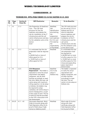
CRRIGENDUM- Webel Technology Limited
修改后,估计应需要:o 40,000平方英尺或更多的CCU办公空间。o 10,000平方英尺或更多的FVU办公空间(在地区级别需要的总估计办公空间)3 14 2.2.5 CCU人力要求 - 预计,预计将验证实际要求和部署人力,以及所有其他设施,因此所有其他设施都可以满足SLAS。虽然要在Kolkata设置具有最大坐姿的主要呼叫中心设置,但作为工作范围的一部分,可能需要投标人在地区总部设置子公司呼叫中心设置。与政府的讨论中,应将地区名单提供给CSP。
技术概要 技术报价详情
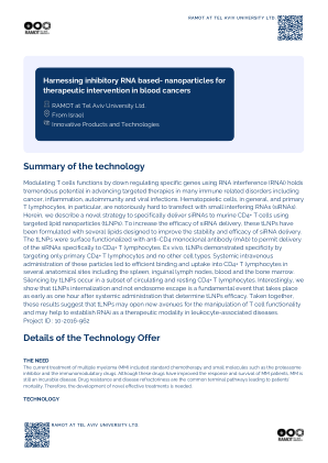
使用 RNA 干扰 (RNAi) 下调特定基因来调节 T 细胞功能,在推进许多免疫相关疾病(包括癌症、炎症、自身免疫和病毒感染)的靶向治疗方面具有巨大潜力。造血细胞,尤其是原代 T 淋巴细胞,通常很难用小干扰 RNA (siRNA) 转染。在此,我们描述了一种使用靶向脂质纳米颗粒 (tLNP) 将 siRNA 特异性地递送到小鼠 CD4+ T 细胞的新策略。为了提高 siRNA 递送的效率,这些 tLNP 已与几种脂质一起配制,旨在提高 siRNA 递送的稳定性和效率。tLNP 表面用抗 CD4 单克隆抗体 (mAb) 功能化,以允许将 siRNA 特异性地递送到 CD4+ T 淋巴细胞。体外,tLNP 通过仅靶向原代 CD4+ T 淋巴细胞而不靶向其他细胞类型表现出特异性。这些粒子的全身静脉内给药导致有效结合并被多个解剖部位的 CD4+ T 淋巴细胞吸收,包括脾脏、腹股沟淋巴结、血液和骨髓。tLNPs 的沉默发生在循环和静息 CD4+ T 淋巴细胞的一个子集中。有趣的是,我们表明 tLNPs 内化而不是内体逃逸是一个基本事件,它早在全身给药后一小时内就发生,决定了 tLNPs 的功效。总之,这些结果表明 tLNPs 可能为操纵 T 细胞功能开辟新途径,并可能有助于建立 RNAi 作为白细胞相关疾病的治疗方式。项目 ID:10-2016-962
采用方名称 2Wire ABIT Computer Corporation Acard Technology Corporation AccFast Technology Corp. Accton Technology Corporation Acer Advanced
采用方名称 2Wire ABIT Computer Corporation Acard Technology Corporation AccFast Technology Corp. Accton Technology Corporation Acer Advanced Lab Achieva Electronics ACON-Advanced connectek Inc. Actisys Corporation ADDMM LLC Addonics Technologies Incorporated ADI Corp. ADMtek Incorporated Advance Modules Advanced Flash Memory Card Technology Co., Ltd. Advanced Micro Devices AGFA-Gevaert NV Agilent Technologies, Inc. AIMEX Corporation AKAI professional MI Corp. Alation Systems, Inc. Alcor Micro Inc. Allion Computer Inc. ALPS Electric Co., Ltd. Altera Corporation Always READY Internet Service Enterprise, LLC (ARISE) American Biometric Company American Computer and Digital Components Ames ADT, Inc./Applied Device Technologies Anchor Chips And-Or Logic Antonio Precise Products Manufactory Ltd. APLUX Communications Ltd. Applied MicroSystems Corporation AppoTech Limited Aptiv Services US, LLC Araneus Information Systems OY Arasan Chip Systems Inc.

数字科技与人工智能Digital Technology ...
新规概览 .................................................................................................................................................................5

Listowel Technology Inc. 业务特色
Listowel Technology Inc. (LTI) 是创新和社区精神的灯塔。从一开始,LTI 就不仅仅是一家企业。它是一个创新与奉献相结合的地方,也是当地劳动力受到重视和赋权的地方。LTI 成立于 1997 年,从一家小型工厂发展成为一家蓬勃发展的企业,拥有约 485 名员工,占地面积 45.4 英亩,运营面积 266,000 平方英尺。