XiaoMi-AI文件搜索系统
World File Search Systemdatasheet
产品数据表
电磁兼容性静电放电免疫测试 - 测试水平:8 kV(空气排放)符合IEC 61000-4-2静电放电免疫测试 - 测试水平:6 kV(接触式放电)符合IEC 61000-4-2 transient/burst immunity test - test level: 2 kV (power lines) conforming to IEC 61000-4-4 Electrical fast transient/burst immunity test - test level: 1 kV (between analogue I/O and operating voltage) conforming to IEC 61000-4-4 Electrical fast transient/burst immunity test - test level: 2 kV (relay wires) conforming to IEC 61000-4-4 Electrical fast transient/burst immunity test - test level: 1 kV (Ethernet line) conforming to IEC 61000-4-4 Electrical fast transient/burst immunity test - test level: 1 kV (COM line) conforming to IEC 61000-4-4 Electrical fast transient/burst immunity test - test level: 1 kV (CAN line) conforming to IEC 61000-4-4 Surge immunity test - test level: 2 kV (power供应(公共模式))符合IEC 61000-4-5激增免疫测试 - 测试水平:1 kV(电源(差异模式))符合IEC 61000-4-4-5激增免疫测试 - 测试水平:1 kV公共模式(数字I/O)符合IEC 61000-4-4-5激增测试测试水平 - 0.5 kV:0.5 kV: 61000-4-5 Conducted RF disturbances - test level: 10 V (0.15...80 MHz) conforming to IEC 61000-4-6 Conducted emission - test level: 150 kHz...30 MHz conforming to EN 55011 Radiated emission - test level: 30 MHz...1 GHz conforming to EN 55011
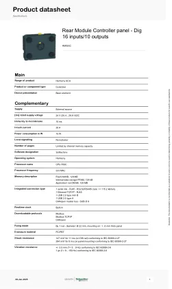
产品数据表
Electromagnetic compatibility Electrostatic discharge 4 kV criteria B contact discharge conforming to IEC 61000-4-2 Electrostatic discharge 8 kV criteria B air discharge conforming to IEC 61000-4-2 Conducted RF disturbances 10 V, 0.15...80 MHz criteria A conforming to IEC 61000-4-6 Radiated radio-frequency electromagnetic field immunity test 10 V/m, 80 MHz...1 GHz criteria A conforming to IEC 61000-4-3 Surge immunity test 1 kV criteria B output ports line to line conforming to IEC 61000-4-5 Surge immunity test 2 kV criteria B output ports line to earth conforming to IEC 61000-4-5 Surge immunity test 1 kV criteria B input ports line to earth conforming to IEC 61000-4-5电气快速瞬态/爆发免疫测试2 KV,5KHz标准B输出端口符合IEC 61000-4-4的免疫力降低电压下降0%/20毫秒的标准B标准B符合IEC 61000-4-11符合IEC 61000-4-11的电压dips 40%/200毫秒40%/200 ms的IEC cormitia cormitia cormitia cormitia cormitia cormitia for IEC 61/200%IMM cormitia for IEC 611000-4-11/tos 611000-4-11/tot tot tot contips 611000-4-11/tot标准c符合IEC 61000-4-11对短中断0%/5 s标准的免疫力C符合IEC 61000-4-11符合IEC 61000-4-11电气快速瞬态/爆发免疫测试1 KV,5KHz标准,标准B输入端口符合IEC 61000-4-4-4-4-4辐射型电视范围3. V/HADED hode five fimber test 3 3 3 3辐射电位3.符合IEC 61000-4-3辐射排放30 ... 1000 MHz环境符合IEC 60947-1进行排放0.15 ... 30 MHz环境A符合IEC 60947-1
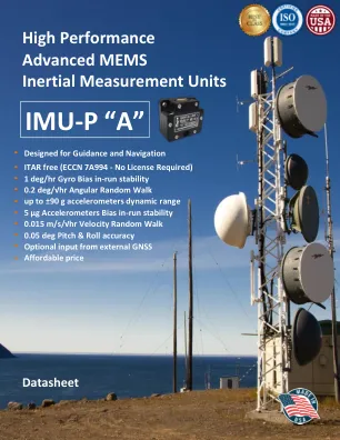
IMU-P数据表
IMU-P IMU-P Tactical Industrial Measurement range deg/sec ±450 / ±950 / ±2000 ±450 / ±950 / ±2000 Bandwidth (-3dB) Hz 260 260 Data update rate Hz 2000 2000 Bias in-run stability (Allan Variance, RMS) deg/hr 1 3 Bias repeatability (turn-on to turn-on, RMS) deg/hr 15 30偏置不稳定性(超过温度范围,RMS)DEG/HR 30 50 SF精度(超过温度范围)PPM 1000 4000噪声。Angular Random Walk (ARW) deg/√hr 0.2 0.3 Non-linearity ppm 100 200 Axis misalignment mrad 0.15 0.3 Accelerometers IMU-P (Tactical) IMU-P (Industrial) Measurement range g ±8 ±15 ±40 ±90 ±8 ±15 ±40 ±90 Bandwidth (-3dB) Hz 260 260 260 260 260 260 260 260偏差运行稳定性(RMS,Allan差异)mg 0.005 0.02 0.02 0.03 1 0.01 0.01 0.03 0.05 1偏差不稳定(温度范围,RMS)mg 0.5 0.7 1.2 200 0.7 1.1 1.1 1.1 1.1 1.1 1.5 200 200偏差一年一年重复性mg 1.3 1.3 1.5 1.5 1.5 200 1.5 200 1.5 200 00 000 500 000 500 000 500 SF精度(超过温度)500 000 500 SF精度2000 SF一年重复性PPM 500 1300 1500 2000 800 1400 1700 2000噪声。Velocity Random Walk (VRW) m/sec/√hr 0.015 0.035 0.045 15 0.02 0.045 0.06 15 Non-linearity ppm 150 150 150 3000 340 800 1000 3000 Axis misalignment mrad 0.15 0.15 0.15 0.3 0.2 0.3 0.3 0.3 Inclinometer IMU-P (Tactical) IMU-P (Industrial) Measurement range, Pitch / Roll deg ±90 / ±180 ±90 / ±180 Resolution deg 0.01 0.01 Static accuracy, RMS deg 0.05 0.05 Dynamic accuracy, RMS deg 0.08 0.08 Environment IMU-P (Tactical) IMU-P (Industrial) Mechanical shock g, s 40, 0.011 half-sine pulse 40, 0.011 half-sine pulse Vibration g, Hz 7, 20 – 2000 7, 20 – 2000 Environmental Protection - IP67 IP67 Operating temperature deg C -40 to +85 -40 to +85 Storage temperature deg C -50 to +90 -50 to +90 Low pressure Pa, min 1750, 30 1750, 30 Humidity % up to 95 up to 95 MTBF (G M @+65degC, operational) hours 100,000 100,000 Life time (operational) years 10 10 Life time (storage) years 17 17 Electrical IMU-P (战术)IMU-P(工业)电源电压V DC 5至30 5至30功耗瓦特0.8 @ 5V 0.8 @ 5V输出接口-RS-422/RS-232/RS-232/RS-485 RS-485 RS-422/RS-422/RS-232/RS-232/RS-485输出数据格式 - binary-Binary-binary 3 33 EMC/EMI/ESD STD-461G STD-461G机械IMU-P(战术)IMU-P(工业)尺寸mm 39 x 45 x 45 x 22 39 x 45 x 45 x 22重量克70 70自定义外壳和连接器自定义可用可用
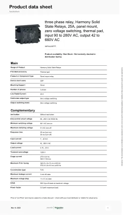
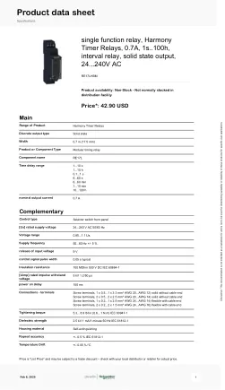
产品数据表
电磁兼容性 静电放电抗扰度试验 - 测试等级: 8 kV (空气放电) 符合 IEC 61000-4-2 静电放电抗扰度试验 - 测试等级: 6 kV (接触放电) 符合 IEC 61000-4-2 电磁场敏感性 - 测试等级: 10 V/m (80 MHz ... 3 GHz) 符合 IEC 61000-4-3 电源频率磁场 - 测试等级: 30 A/m 符合 IEC 61000-4-8 电气快速瞬变/突发抗扰度试验 - 测试等级: 2 kV (电源线) 符合 IEC 61000-4-4 电气快速瞬变/突发抗扰度试验 - 测试等级: 2 kV (继电器输出) 符合 IEC 61000-4-4 电气快速瞬变/突发抗扰度试验 - 测试等级: 1 kV (I/O) 符合 IEC 61000-4-4 电快速瞬变/突发抗扰度试验 - 测试等级: 1 kV (串行链路) 符合 IEC 61000-4-4 1.2/50 µs 冲击波抗扰度试验 - 测试等级: 1 kV (电源线 (DC)) 符合 IEC 61000-4-5 1.2/50 µs 冲击波抗扰度试验 - 测试等级: 2 kV (电源线 (AC)) 符合 IEC 61000-4-5 1.2/50 µs 冲击波抗扰度试验 - 测试等级: 2 kV (继电器输出) 符合 IEC 61000-4-5 1.2/50 µs 冲击波抗扰度试验 - 测试等级: 1 kV (I/O) 符合 IEC 61000-4-5 1.2/50 µs 冲击波抗扰度试验 - 测试等级: 1 kV (屏蔽电缆) 符合 IEC 61000-4-5 1.2/50 µs 冲击波抗扰度试验 - 测试等级: 0.5 kV (电源线 (DC)) 符合 IEC 61000-4-5 1.2/50 µs 冲击波抗扰度试验 - 测试等级: 1 kV (电源线 (AC)) 符合 IEC 61000-4-5 传导 RF 干扰 - 测试等级: 10 V (0.15...80 MHz) 符合 IEC 61000-4-6 传导发射 - 测试等级: 79 dBμV/m QP/66 dBμV/m AV (电源线 (AC)) 符合 IEC 55011 传导发射 - 测试等级: 73 dBμV/m QP/60 dBμV/m AV (电源线 (AC)) 符合 IEC 55011 辐射发射 - 测试等级: 40 dBμV/m QP A 级(10 m) 符合 IEC 55011 辐射发射 - 测试等级: 47 dBμV/m QP A 类 (10 m) 符合 IEC 55011

FortiSASE 数据表
FortiSASE 使组织能够授予每个用户和每个会话对 Web、云和应用程序的安全访问权限,无论它们部署在何处,并结合完全集成的企业级安全性。通过安全性和网络之间的无缝融合,FortiSASE 可确保将相同级别的保护、可见性和用户体验扩展到任何地方的每个用户。对于那些注重合规性的人来说,FortiSASE 已通过服务组织控制 (SOC2) 认证,该认证提供独立验证,确保解决方案安全控制符合美国注册会计师协会 (AICPA) 适用的信托服务原则和标准。此 SOC 2、Type II 标准认证表明我们致力于确保我们的客户能够满足各种合规性要求。Fortinet 提供 99.999% 的 SLA 和延迟保证,用于安全检查,这是因为其在全球范围内拥有数百个安全 PoP。
RP2040 数据表
2.1.1. AHB-Lite Crossbar . . . . . . . . . . . . . . . . . . . . . . . . . . . . . . . . . . . . . . . . . . . . . . . . . . . . . . . . . . . . . . . . . . . . . . . . . . . . . . . . . . . . . . . . . . . . . . . . . . . ....................................................................................................................................................................................................................... 17 2.1.3. APB 桥....................................................................................................................................................................................................................... ........................................................................................................................................................................................ ........................................................................................................................................................................ ........................................................................................................................................................................................ ........................................................................................................................................................................................ ........................................................................................................................................................................................ ........................................................................................................................................................................................ 17 2.1.4. 窄 IO 寄存器写入.................... ... ....................................................................................................................................................................................................................................... 18 2.2. 地址映射....................................................................................................................................................................................................... ....................................................................................................................................................................... ....................................................................................................................................................................... ....................................................................................................................................................................... ....................................................................................................................................................................................... ....................................................................................................................................................................................... ....................................................................................................................................................................................... ...24
产品数据表
电磁兼容性 静电放电抗扰度试验 6 kV(接触) 级别 3 IEC 61000-4-2 静电放电抗扰度试验 8 kV(空气中) 级别 3 IEC 61000-4-2 电磁场敏感性 10 V/m(80 MHz 至 1 GHz) 级别 3 IEC 61000-4-3 电气快速瞬变/脉冲群抗扰度试验 1 kV 电容式连接夹) 级别 3 IEC 61000-4-4 电气快速瞬变/脉冲群抗扰度试验 2 kV 直接) 级别 3 IEC 61000-4-4 1.2/50 µs 冲击波抗扰度试验 1 kV 差模) 级别 3 IEC 61000-4-5 1.2/50 µs 冲击波抗扰度试验 2 kV 共模) 级别 3 IEC 61000-4-5 传导 RF 干扰 10 V 0.15 ...80 MHz 3 级 IEC 61000-4-6 电压暂降和中断抗扰度试验 0 % 1 个周期) IEC 61000-4-11 电压暂降和中断抗扰度试验 70 % 25/30 个周期) IEC 61000-4-11 传导和辐射发射 B 级 EN 55022