XiaoMi-AI文件搜索系统
World File Search Systemwavelength
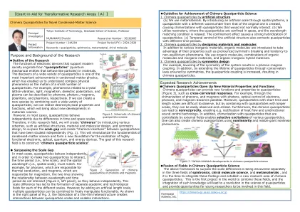
支持 NASA 空间通信和导航计划的地面站 1 概述
恒定面积抛物面天线和反射镜的远场角波束宽度与发射信号的波长成正比。因此,天线或透镜的发射信号功率分布在与波长平方成正比的立体角上,即到达接收器的信号功率与频率平方成正比。对于给定的发射孔径尺寸,频率越高,到达接收器的信号功率越大。接收器噪声也会随着频率的增加而增加。在光频率下,与频率成正比的量子噪声占主导地位。在射频下,量子噪声微不足道:其他不随频率强烈变化的噪声源占主导地位。因此,首先,接收器噪声与频率成正比。由于接收信号功率与频率平方成正比,接收器信噪比 (SNR) 与频率成正比。无差错通信的最大可能速率会随着接收的 SNR 而增加。这是光通信的主要优势。迄今为止,NASA 使用的最高下行射频通信频率是深空 Ka 波段下行频率 32 千兆赫 (GHz)。典型的下行光波长为 1550 纳米 (nm),相当于 193.5 太赫兹 (THz) 的频率。因此,光与射频频率之比为 193.5 THz/32 GHz,约为 6000。在其他所有条件相同的情况下,1550 nm 光通信系统的接收器 SNR 有可能比 Ka 波段系统高 6000 倍。
文章的柔性指导模式共振的理论研究是通过将银纳米颗粒嵌入聚合物矩阵中的应变感应应用的
2 Opto-Electrochemical Sensing Research Team (OEC), Spectroscopic and Sensing Devices Research Group (SSDRG), National Electronics and Computer Technology Center (NECTEC), Pathum Thani 12120, Thailand E-mail: a pundharika.n@gmail.com, b sakoolkan.boonruang@nectec.or.th, c,* wsoliman@gmail.com(通讯作者)摘要。本文介绍了柔性引导模式共振(GMR)结构的理论分析,其配置具有增强的折射率聚合物纳米复合材料,其中涂有原始聚合物制成的铸造或烙印的银纳米颗粒。控制嵌入式纳米颗粒(NP)的体积分数和膜厚度都调整了设备灵敏度,以用于在机械横向应变检测中应用。工作引入了在有效索引中修改散射矩阵方法(SMM)的使用,以准确预测共振波长峰。结果显示了与严格的耦合波分析(RCWA)的良好一致性,尤其是对于基本指导模式和衍射之间的相位匹配条件。灵敏度是通过横向应变引起的光栅周期来计算的,并将其与产生的波长偏移相关。使用SMM进行共振波长计算,将计算成本降低了144倍,同时与RCWA和有限差频域方法(FDFDM)保持了良好的一致性。关键字:柔性指南模式共振(GMR),嵌入式纳米颗粒(NP),散射矩阵方法(SMM),严格的耦合波分析(RCWA)。
用于量子计算的集成光子学
Cegielski, Piotr J. 等人。“用于 OCT 应用的氮化硅波导和光斑尺寸转换器,在 1010 nm 至 1110 nm 的宽波长范围内损耗小于 1.76 dB。”《ECIO》(2020 年)

通过收购 NKT Photonics 推进增长战略
通过将 NKT Photonics 的先进光纤激光技术添加到 Hamamatsu Photonics 的光检测技术中,我们获得了光子学中所有必要的技术(可以控制光的所有参数,例如波长、相位、亮度和灵敏度)
研究变性和重新结合的方法...
由于核苷酸的杂环,核酸会吸收紫外线 (UV) 光;糖磷酸骨架对吸收没有贡献。DNA 和 RNA 的最大吸收波长均为 260nm (λmax = 260nm),每个碱基都有一个特征值。
Nanophotonics: shrinking light-based technology
Abstract The study of light at the nanoscale has become a vibrant field of research, as researchers now master the flow of light at length scales far below the optical wavelength, largely surpassing the classical limits imposed by diffraction. Using metallic and dielectric nanostructures precisely sculpted into 2D and 3D nanoarchitectures, light can be scattered, refracted, confined, filtered, and processed in fascinating new ways, impossible to achieve with natural materials and in conventional geometries. This control over light at the nanoscale has not only unveiled a plethora of new phenomena, but has also led to a variety of relevant applications, including new venues for integrated circuitry, optical computing, solar, and medical technologies, setting high expectations for many novel discoveries in the years to come. Introduction Optics and the science of light is a lively field of research that continues to surprise decade after decade with fundamental breakthroughs and disruptive applications. Communications technology has been revolutionized by the invention of the laser and the optical fiber, incandescent light bulbs are being replaced by efficient solid-state lighting, and solar energy technologies are on their way to price parity with fossil-fuel based power generation. A large number of these developments has resulted from increased control over the flow of light at length scales smaller than the wavelength. Squeezing light to nanoscale dimensions also opens the prospect of dense optical integrated circuits, which may overcome fundamental challenges related to bandwidth and energy dissipation in today's electronic integrated circuit technology. More broadly, the field of nanophotonics aims at overcoming Abbe's diffraction limit, developing technology able to manipulate light on a deep- subwavelength scale. As photons are shrunk to the nanometer scale, ultimately approaching the scale of the wave function of electrons, fundamental new science is expected, and important technological advances appear. In this article we review recent highlights in the science and applications of nanophotonics, focusing on the ultraviolet/visible/near-infrared spectral range, and provide an outlook for the bright future of this research field. Photonic crystals The initial concept for on-chip miniaturization of light dates back to the late 1990's, when photonic crystals – periodic structures fabricated from high refractive index materials like Si or GaAs – were proposed and realized (Fig. 1A). As the periodicity in these structures approaches the wavelength of light a photonic bandgap can appear, analogous to the energy bandgap in a semiconductor. The propagation of light with a frequency in the band gap is then forbidden, except in localized regions created by a well-designed break in periodicity, such as line defects that can guide light, or point defects that confine light. Band structure engineering gives exquisite control over light dispersion, i.e., over the relation between its frequency ω and its effective propagation constant k=2 π/λ, and thereby also over how fast signals of different wavelengths propagate, as given by the group velocity d ω /dk.
创新光学和无线网络全球...
为了满足 IOWN 用例的极端带宽和延迟要求,IOWN GF 定义了一个名为开放全光子网络 (APN) 的新网络,并于 2022 年初发布了其 Release 1 架构文档。APN 是一个基于波长交换的面向连接的网络,支持各种物理部署场景,包括在客户场所部署波长复用/交换节点的场景。这种部署灵活性来自 APN 的开放和分解架构,它定义了三个功能组件,分别是 APN-T(收发器)、APN-G(网关)和 APN-I(交换)。通过在通信端点之间动态创建光波长连接,APN 实现了非常高的速度和非常低的延迟的数据传输,例如数十/数百 Gbps 和不到一毫秒。通过这种方式,APN 将有效且高效地支持 IOWN GF 用例。
真空密封硅光子 MEMS 可调环形谐振器,具有对耦合和相位的独立控制
摘要:环形谐振器是硅光子学中滤波器、光延迟线或传感器的重要元件。然而,目前工厂中还没有低功耗的可重构环形谐振器。我们展示了一种使用低功耗微机电 (MEMS) 驱动独立调节往返相位和耦合的加/减环形谐振器。在波长为 1540 nm 且最大电压为 40 V 的情况下,移相器提供 0.15 nm 的谐振波长调谐,而可调耦合器可以将直通端口处的光学谐振消光比从 0 调节到 30 dB。光学谐振显示出 29 000 的被动品质因数,通过驱动可以增加到近 50 000。MEMS 环在晶圆级上单独真空密封,能够可靠且长期地保护免受环境影响。我们循环机械致动器超过 4 × 10 9
量子力学基础 - 古典观点
黑体辐射 • 黑体辐射的能量并不是由所有波长的光均匀共享的。 • 黑体辐射的光谱表明某些波长比其他波长获得更多的能量。 • 显示了三种不同温度的三种光谱。 • 以下是有关黑体辐射的一些实验事实:1. 黑体光谱仅取决于物体的温度,而不取决于材料的类型,即,如果温度相同,所有材料都会发射相同的黑体光谱。2. 随着物体温度的升高,它会在所有波长下发射更多的黑体能量。3. 随着物体温度的升高,黑体光谱的峰值波长向更短的波长移动。例如,蓝色恒星比红色恒星更热。4. 黑体光谱总是在左侧(短波长、高频侧)变小。