XiaoMi-AI文件搜索系统
World File Search SystemOrbotech
奥宝科技 Precise™ 800
* 其他层压板需要由 KLA 测试 ** 较大尺寸的短路可在聚合模式下成形 *** 基于带有 FR4 层压板的测试面板,包括 L/U **** 取决于缺陷数量和分布 ***** 取决于导体的尺寸、方向和厚度。Orbotech Precise Stick 消耗量可能存在很大差异。
融合22
Detected Defects Shorts, opens, minimum line/space violations, nicks, protrusions, dishdowns, copper splashes, pinholes, missing or excess features, wrong size and position of features, clearance and split plane violations, blocked holes, annular ring violations, SMT violations, black spots, wire bonding pad defects, flip chip pad defects, defects in through blind vias
Orbotech Ultra Fusion™200
Detected Defects Shorts, opens, minimum line/space violations, nicks, protrusions, dishdowns, copper splashes, pinholes, missing or excess features, wrong size and position of features, clearance and split plane violations, blocked holes, annular ring violations, SMT violations, black spots, wire bonding pad defects, flip chip pad defects, defects in through blind vias
Ultra Filter 700
Shorts, opens, minimum line/space violations, nicks, protrusions, dish downs, copper splashes, pinholes, missing or excess features, wrong size and position of features, clearance and split plane violations, blocked holes, annular ring violations, SMT violations, black spots, wire bonding pad defects, flip chip pad defects, laser via defects as missing drill, over drill, under drill, via shift, residue在Via中,通过大小和形状
超大300
Detected Defects Shorts, opens, minimum line/space violations, nicks, protrusions, dishdowns, copper splashes, pinholes, missing or excess features, wrong size and position of features, clearance and split plane violations, blocked holes, annular ring violations, SMT violations, black spots, wire bonding pad defects, flip chip pad defects, defects in through blind vias
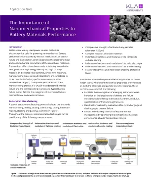
电池材料的纳米构件-KLA仪器
KLA服务从工具安装和系统优化到生产率增强和全球供应链管理,KLA服务是全球客户的可信赖合作伙伴 - 提供了专注于最大化工具性能和可用性的无与伦比的体验。©2023 KLA Corporation。全球保留的所有权利。KLA保留更改硬件和/或软件规格的权利,恕不另行通知。所有品牌或产品/服务名称可能是其各自所有者的商标,包括但不限于:KLA,Orbotech。