机构名称:
¥ 1.0
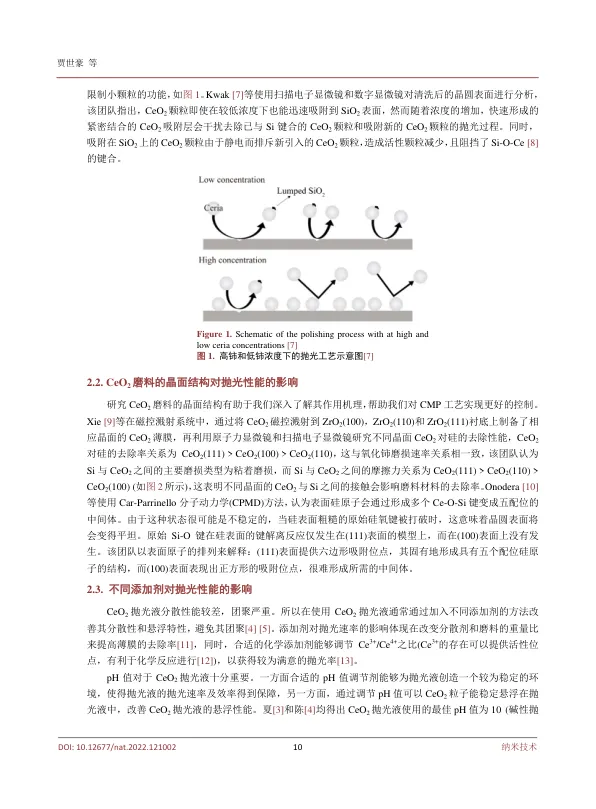
Figure 7. Morphologies and surface roughness values of (a) the initial surface and the polished surface under conditions of (b) without UV-light, (c) TiO 2 film electrode with UV-light, (d) TiO 2 film electrode with UV-light and anodic bias, (e) CeO 2 -TiO 2 composite-film electrode with UV-light and (f) CeO 2 -TiO 2 composite-film elec- trode with UV-light and anodic bias [31] 图 7. (a) 初始表面; (b) 无紫外光条件下抛光表面; (c) 有紫外光并使用用 TiO 2 薄膜电极抛光下表 面; (d) 在有紫外光和阳极偏压的 TiO 2 薄膜电极下抛光表面; (e) 有紫外光并使用 CeO 2 -TiO 2 复合 膜电极下抛光表面; (f) 有紫外光和阳极偏压的 CeO 2 -TiO 2 复合膜电极抛光表面的形貌和表面粗糙 度值 [31]
用于元件抛光的CeO2基复合材料的研究进展
主要关键词

相关文件推荐