机构名称:
¥ 1.0
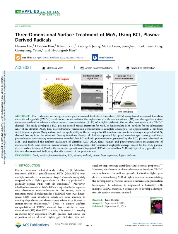
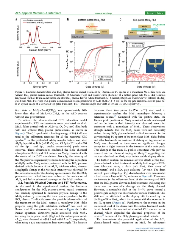
ABSTRACT: The realization of next-generation gate-all-around field-effect transistors (FETs) using two-dimensional transition metal dichalcogenide (TMDC) semiconductors necessitates the exploration of a three-dimensional (3D) and damage-free surface treatment method to achieve uniform atomic layer-deposition (ALD) of a high-k dielectric film on the inert surface of a TMDC channel.这项研究开发了对MOS 2的BCl 3等离子体衍生的自由基处理,以使MOS 2表面功能化,以使超薄AL 2 O 3膜的随后ALD函数。微观结构验证证明,在平面MOS 2表面上大约2 nm厚2 O 3膜的覆盖范围,并使用从基板漂浮的悬浮的MOS 2通道确认了该技术对3D结构的适用性。密度功能理论计算由光学发射光谱和X射线光电子光谱测量值支撑,揭示了Bcl激进分子主要由BCL 3等离子体产生,并吸附在MOS 2上,并促进了Ultrathin Ald-Ald Ald-Ald 2 O 3膜的均匀成核。拉曼和单层MOS 2的光致发光测量以及底部门控的FET的电测量结果证实,由Bcl 3等离子体衍生的自由基治疗造成的可忽略不计。最后,证明了具有超薄ALD-Al 2 O 3(〜5 nm)栅极介电膜的顶部门控FET的成功操作,表明预处理的有效性。关键字:MOS 2,表面功能化,BCl 3等离子体,自由基,原子层沉积,高K介电
使用Bcl3等离子体衍生的自由基对MOS2进行三维表面处理
主要关键词


相关文件推荐